- 您现在的位置:买卖IC网 > Sheet目录484 > NP100P06PDG-E1-AY (Renesas Electronics America)MOSFET P-CH -60V MP-25ZP/TO-263
DATA SHEET
MOS FIELD EFFECT TRANSISTOR
NP100P06PDG
SWITCHING
P-CHANNEL POWER MOSFET
DESCRIPTION
The NP100P06PDG is P-channel MOS Field Effect Transistor designed for high current switching applications.
<R>
ORDERING INFORMATION
PART NUMBER
NP100P06PDG-E1-AY
Note
LEAD PLATING
PACKING
PACKAGE
NP100P06PDG-E2-AY
Note
Pure Sn (Tin)
Tape 800 p/reel
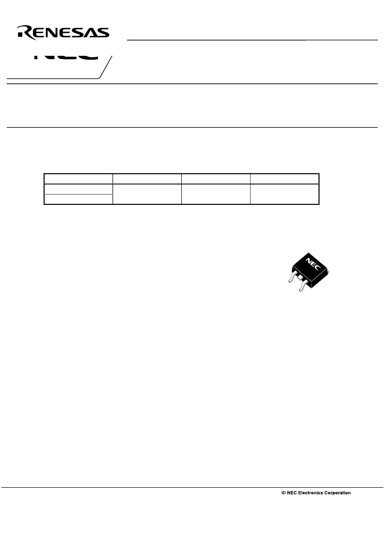
TO-263 (MP-25ZP)
Note Pb-free (This product does not contain Pb in external electrode.)
FEATURES
? Super low on-state resistance
R DS(on)1 = 6.0 m Ω MAX. (V GS = ? 10 V, I D = ? 50 A)
R DS(on)2 = 7.8 m Ω MAX. (V GS = ? 4.5 V, I D = ? 50 A)
? High current rating: I D(DC) = m 100 A
ABSOLUTE MAXIMUM RATINGS (T A = 25 ° C)
(TO-263)
Drain Current (pulse)
Drain to Source Voltage (V GS = 0 V)
Gate to Source Voltage (V DS = 0 V)
Drain Current (DC) (T C = 25 ° C)
Note1
Total Power Dissipation (T C = 25 ° C)
Total Power Dissipation (T A = 25 ° C)
Channel Temperature
Storage Temperature
V DSS
V GSS
I D(DC)
I D(pulse)
P T1
P T2
T ch
T stg
? 60
m 20
m 100
m 300
200
1.8
175
? 55 to + 175
V
V
A
A
W
W
° C
° C
Single Avalanche Current
Single Avalanche Energy
Note2
Note2
I AS
E AS
64
420
A
mJ
Notes 1. PW ≤ 10 μ s, Duty Cycle ≤ 1%
2. Starting T ch = 25 ° C, V DD = ? 30 V, R G = 25 Ω , V GS = ? 20 → 0 V
THERMAL RESISTANCE
Channel to Case Thermal Resistance
Channel to Ambient Thermal Resistance
R th(ch-C)
R th(ch-A)
0.75
83.3
° C/W
° C/W
The information in this document is subject to change without notice. Before using this document, please
confirm that this is the latest version.
Not all products and/or types are available in every country. Please check with an NEC Electronics
sales representative for availability and additional information.
Document No. D18693EJ3V0DS00 (3rd edition)
Date Published May 2007 NS CP(K)
Printed in Japan
The mark <R> shows major revised points.
The revised points can be easily searched by copying an "<R>" in the PDF file and specifying it in the "Find what:" field.
2007
发布紧急采购,3分钟左右您将得到回复。
相关PDF资料
NP100P06PLG-E1-AY
MOSFET P-CH -60V MP-25ZP/TO-263
NP109N04PUJ-E1B-AY
MOSFET N-CH 40V MP-25ZP/TO-263
NP109N055PUJ-E1B-AY
MOSFET N-CH 55V MP-25ZP/TO-263
NP110N03PUG-E1-AY
MOSFET N-CH 30V MP-25ZP/TO-263
NP110N04PDG-E1-AY
MOSFET N-CH 40V MP-25ZP/TO-263
NP110N04PUG-E1-AY
MOSFET N-CH 40V MP-25ZP/TO-263
NP110N04PUJ-E1B-AY
MOSFET N-CH 40V MP-25ZP/TO-263
NP110N055PUG-E2-AY
MOSFET N-CH 55V MP-25ZP/TO-263
相关代理商/技术参数
NP100P06PDG-E1-AZ
制造商:Renesas Electronics Corporation 功能描述:
NP100P06PDG-E2-AY
制造商:NEC 制造商全称:NEC 功能描述:MOS FIELD EFFECT TRANSISTOR
NP100P06PLG
制造商:Renesas Electronics Corporation 功能描述:
NP100P06PLG-E1-AY
功能描述:MOSFET P-CH -60V MP-25ZP/TO-263 RoHS:是 类别:分离式半导体产品 >> FET - 单 系列:- 标准包装:1,000 系列:MESH OVERLAY™ FET 型:MOSFET N 通道,金属氧化物 FET 特点:逻辑电平门 漏极至源极电压(Vdss):200V 电流 - 连续漏极(Id) @ 25° C:18A 开态Rds(最大)@ Id, Vgs @ 25° C:180 毫欧 @ 9A,10V Id 时的 Vgs(th)(最大):4V @ 250µA 闸电荷(Qg) @ Vgs:72nC @ 10V 输入电容 (Ciss) @ Vds:1560pF @ 25V 功率 - 最大:40W 安装类型:通孔 封装/外壳:TO-220-3 整包 供应商设备封装:TO-220FP 包装:管件
NP100P06PLG-E2-AY
制造商:NEC 制造商全称:NEC 功能描述:MOS FIELD EFFECT TRANSISTOR
NP100V105M5X11
制造商:SPC Multicomp 功能描述:CAPACITOR N/P 1UF 100V 制造商:SPC Multicomp 功能描述:CAPACITOR, N/P, 1UF, 100V 制造商:SPC Multicomp 功能描述:CAPACITOR ALUM ELEC, 1UF, 100V, RADIAL; Product Range:MULTICOMP - NP Series; Capacitance:1F; Capacitance Tolerance: 20%; Voltage Rating:100V; Diameter:5mm; Height:11mm; Capacitor Terminals:Radial Leaded; Lead Spacing:2mm ;RoHS Compliant: Yes
NP100V106M8X11.5
制造商:SPC Multicomp 功能描述:CAPACITOR N/P 10UF 100V 制造商:SPC Multicomp 功能描述:CAPACITOR, N/P, 10UF, 100V 制造商:SPC Multicomp 功能描述:CAPACITOR ALUM ELEC, 10UF, 100V, 20%, RADIAL; Product Range:MULTICOMP - NP Series; Capacitance:10F; Capacitance Tolerance: 20%; Voltage Rating:100V; Diameter:8mm; Height:11.5mm; Capacitor Terminals:Radial Leaded; Lead Spacing:3.5mm;RoHS Compliant: Yes
NP100V107M16X25
制造商:SPC Multicomp 功能描述:CAPACITOR N/P 100UF 100V 制造商:SPC Multicomp 功能描述:CAPACITOR, N/P, 100UF, 100V 制造商:SPC Multicomp 功能描述:CAPACITOR, N/P, 100UF, 100V ;ROHS COMPLIANT: YES 制造商:SPC Multicomp 功能描述:CAPACITOR, N/P, 100UF, 100V; Product Range:MULTICOMP - NP Series; Capacitance:100F; Capacitance Tolerance: 20%; Diameter:16mm; Height:25mm; Capacitor Terminals:Radial Leaded; Lead Spacing:7.5mm; Life Time @ Temperature:2000 hours @;RoHS Compliant: Yes
